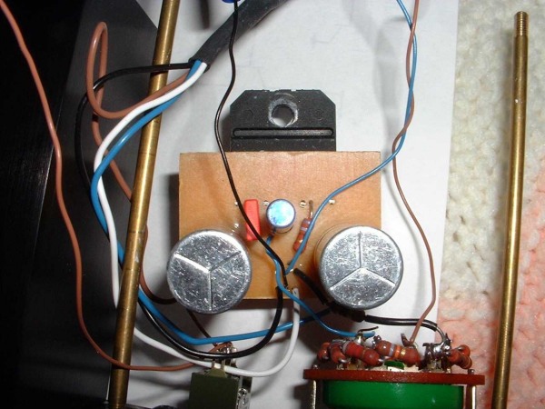
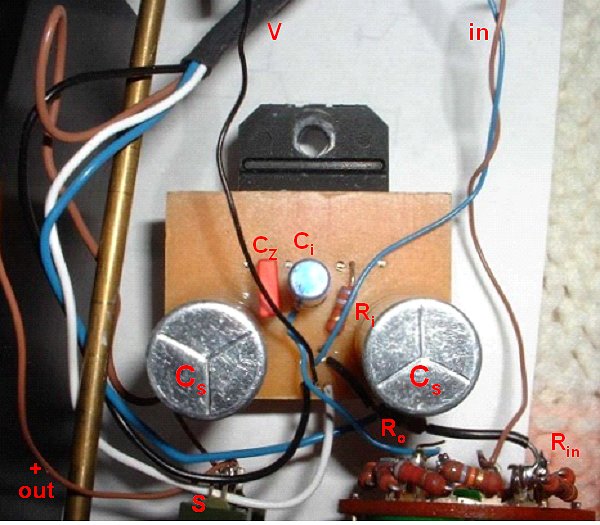
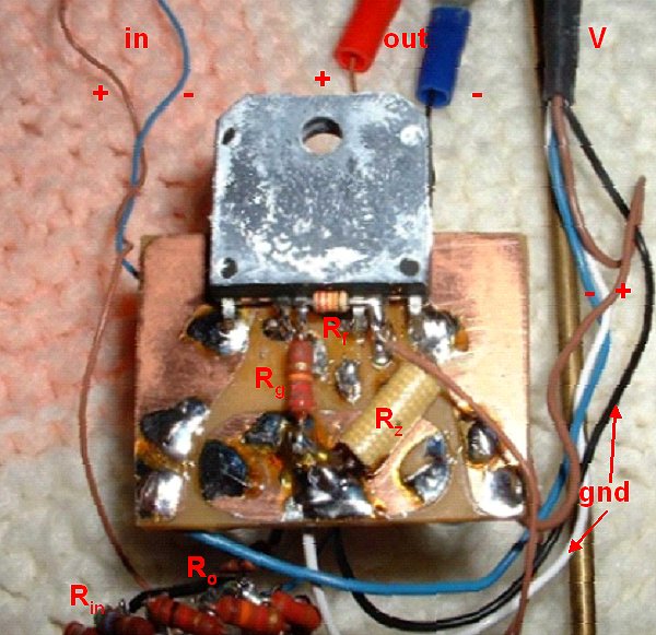
Analysis of the pictures of the Gaincard innards

by Mick Feuerbacher, October 2005.


In 2002 in a thread in Audio Asylum some pictures were presented that were said to show the inside of an original Gaincard. Shortly thereafter Yoshi Segoshi of Sakura Systems responded, claiming that the photos were not of a 47 Labs Gaincard and when asked to provide photos of the internals of a real Gaincard, he refused to do so. Recently, some new images occurred in a 6moons review of the Gaincard. These images showed a very similar board with similar looking components and soldering style, similar cables and connectors and a similar stepped attenuator. These pictures were officially provided by the manufacturer. Comparing the old images with the new ones, I am now quite convinced that the images shown on Audio Asylum were showing the inside of the real Gaincard.

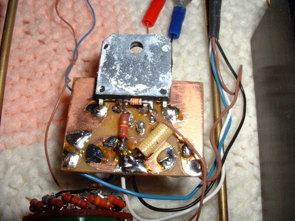
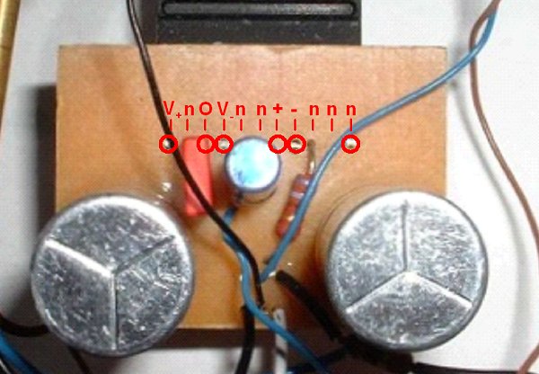
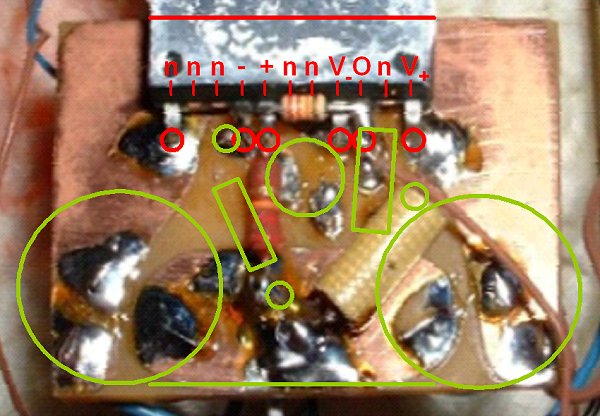
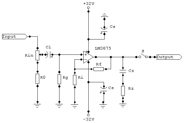
I carefully analyzed them in order to deduce the parts and schematic used for the original Gaincard. Most probably this has been done by millions of DIYers out there before, but I could not find the information in the internet. Maybe my findings are interesting for others as well, so I present them here. I am open for discussions, of course. If you don't agree with my conclusions or want to add something, please contact me (m at dogbreath dot de) ....


The first of the images appearing in the Audio Asylum thread. It was said that the pictures were taken by Craig Fraser. I hope he does not mind that I use them here.

This is the top side of the board with the two skinned supply bypassing caps. On the bottom of the picture the 12 position stepped attenuator with the green switch is seen.


The second image, showing the bottom side of the board.


Rectified image with the connectors labelled. The chip is a national LM3875. O: output; +: pos input; -: neg input; V+ and V-: pos and neg supply; n: not connected.


Bottom of the PCB with connectors labelled. In green are shown the locations (and connections) of the parts located on the front of the board.

The non-connected pins are cut off, only pin 11 (left) was left in order to fix the chip and make a connection to V-. There must be a bridge from pin 11 to pin 4 (V-) under the chip. The Resistor on the top side of the board (previous image) goes through a hole at the position of pin 3 and is bent to connect to the negative input.

There is only one ground on the board, the copper area in the front of the image. No separation of power and signal ground is made.


By careful inspection of the images I have deduced the schematic used. It is a non-inverted rather minimalistic approach. The number of parts, excluding the attenuator and R0, is nine as claimed by the manufacturer.

Although the design is non-inverted, a DC blocker cap is used at the input. I am surprised to see that they used an electrolytic here.

Resistor R0 extends the range of volume control by one step (Thanks Stabist!). This is on the cost of the fully attenuated position. You have to use mute switch for total silence.

A Zobel network is used on the output.

The switch is not a power switch. It simply disconnects the output from the speakers.


What is what on the pictures...

The labels shown are identical to those used in the schematic above.


Indeed, if you scale the image and calculate the length of the signal path (if you do not include the Zobel and Rg) you arrive at something close to 32 mm, as 47 labs claims for the Gaincard.


The values of the resistors are: Rg: 22k, Rf: 22k, Ri: 680. The gain is 33. All resistors seem to be carbon film types. Tolerance is 5 %.

There is no way to identify R0 or the capacitor values. At least, we can determine the dimensions of the components. The Cs caps have a diameter of 15 mm, Ci of 5.4 mm, the dimensions of Cz are 2.6 mm x 7.5 mm. Judging by the color, they may have used a WIMA 100 nF polyester cap for Cz. 100 nF is the value specified in the LM3886 datasheet and the WIMA measures 2.5 mm x 7.2 mm, which fits very well. Maybe someone can identify the makes of the other caps according to their size (let me know if you do). The value of the Cs caps is 1000 uF for the 25 + 25 W version and 2200 uF for the 50 + 50 W version.


The PSU (Power Humpty)

This information was collected from other sources in the internet. The Power Humpty contains a high quality non-toroidal 170 VA transformer. Secondaries are 23.5V, 3.6 A. There are only four diodes, used for the positive and negative rails. The diodes are FE5D 9808 (General Semiconductors). There are no capacitors in the Power Humpty. The ground connections of the positive and negative rail are separately led to the amp boards.