Modifiying the output stage of the Sony Playstation SCPH100x
by Mick Feuerbacher, December 2005. Updated June 2006.
This article describes modifications of the output stage of a PS1 SCPH 100x, which lead to a significant improvement of the sound. The procedures described are, in contrast to the other articles presented, not a result of my own research. They were developed in a combined effort of the users Antoine Deschênes (aka Dragonmaster, who did a major part of the research), Jonathan Ives (Jives11), George Backousis (back), and myself in a thread in the diyaudio.com forum in November and December 2005. Thank you very much, gentlemen, for the very pleasant dissemination of the circuit. It was (and still is) a great pleasure to discuss with you! For those readers that want to increase the sonic performance quite a bit without having to make irreversible modifications to the circuit, even without having to open the case, please have a look at this article on the use of the AV Multi out. Edit: In the updated version of this article I have repeated the modification of the output stage using shielded wires. Some images have been exchanged correspondingly. |
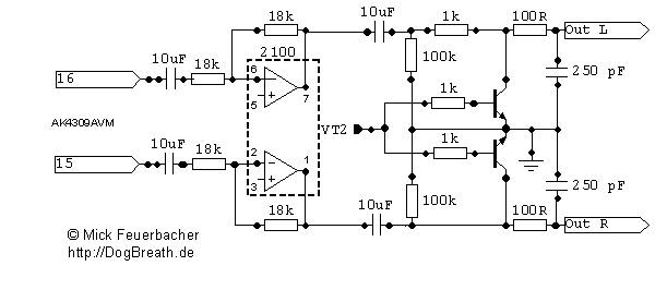
1: Schematic This is the schematic of the DAC input and output stage, which is frequently found on the web. I found it on http://methe-family.de, but I don't know where it originally comes from. The output circuit, i.e. the part on the right after the AOUTL and AOUTR pins of the DAC, are only shown for the AV Multi out (the generic connector on the right side of the rear plate, seen from the back). The RCA out circuit, which is present in the SCPH100x, is not included.
|
The RCA output circuit as deduced by Antoine Deschênes (only some small changes from my side) is shown in this schematic. In the SCPH100x, this circuit is parallel to the one for the Multi AV out shown above. In particular the output stage connected to the RCA jacks is not included. The circuit is similar to that for the AV multi out but the signal goes through an additional opamp (NJM2100) and a second pair of capacitors.
|
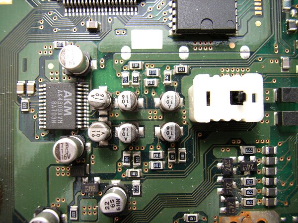
2: Location of the parts on the board The image shows the RCA and AV Multi output stages. To find this area on the board look for the cover safety switch which is seen on the right in the image. On the left you see the DAC, which is a AKM4309AVM. The rear of the PS1 is on the right side of the image. |
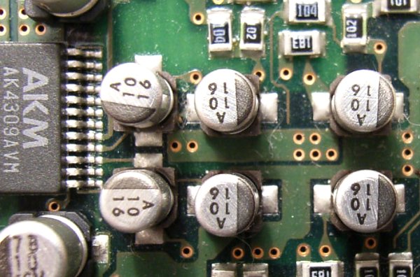
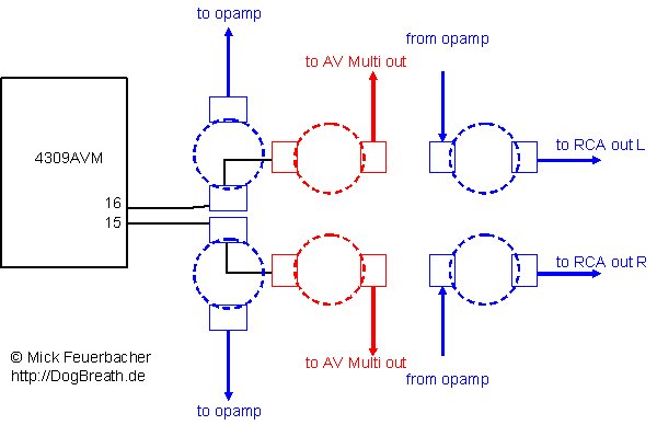
Magnification of the central area of the previous image. Six electrolytic capacitors make up the central part. These are the DC blocking caps of the RCA output (first and third pair) and the AV Multi out (second pair). The caps are connected to pins 15 (right) and 16 (left) of the DAC. |
Connections and locations of the capacitors. All parts and connections of the RCA output circuit are shown in blue, those of the AV Multi out in red. |
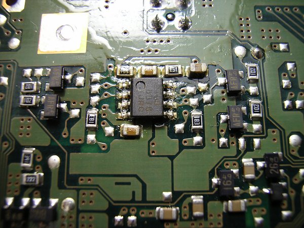
The bottom of the PCB with the NJM2100 opamp and the muting transistors of the AV Multi out and the RCA out. The rear of the PS1 is at the top of the image. |
|
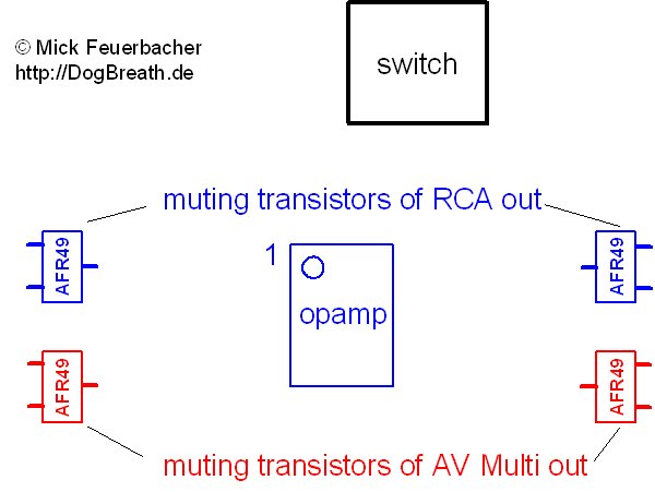
Scheme of the above image showing the most important parts. |
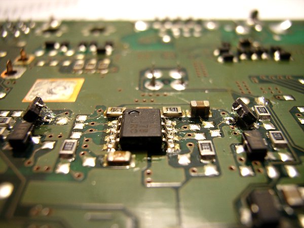
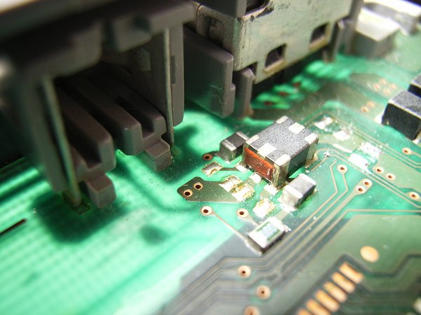
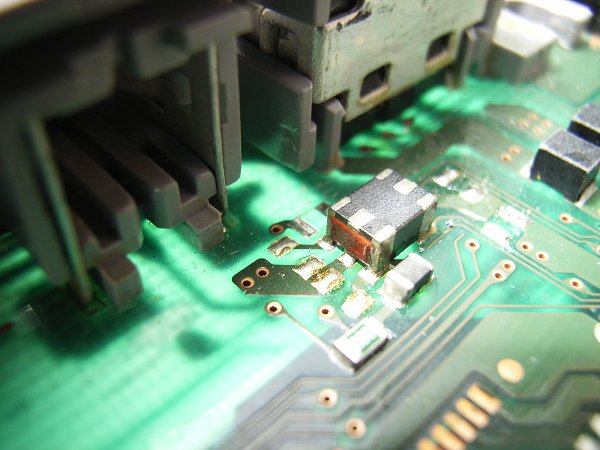
3: Modifications of the output stage Removing the muting transistors from the signal path: The single leg of the muting transistors is the collector. According to the schematic it connects to the output signal between the 1k and the 100R resistors. The transistors can be removed from the signal path by simply lifting the side with the single leg. Put a small screwdriver blade under the transistor, heat the solder junction and lift. Of course you can also remove the transistors completely by desoldering the other two legs too. The image shows a situation where the muting transistors of the RCA output are lifted while those of the AV Multi out are still in the signal path. |
|
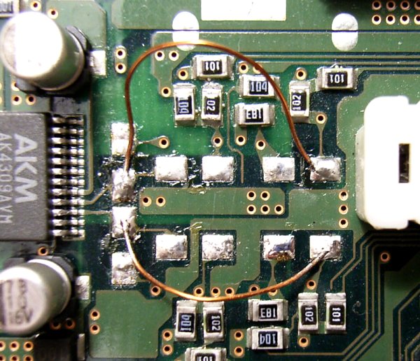
Removing the DC blocking caps: Here the blocking caps of the RCA output (first and third pair) and of the AV Multi out (second pair) are removed. The signal path is closed then by soldering a jumper wire from the input pads of the first set of caps to the output pads of the third pair of caps. You may have problems with DC if the stage following your PS1 has no input blocking capacitors. In that case you can replace the jumper wire by a capacitor. Jonathan Ives has successfully used a bipolar 100uF capacitor (Nitai) here. These two modifications will lead to a significant decrease of components in the signal path and distinct improvements in sound qualitiy have been reported by those who tried it. |
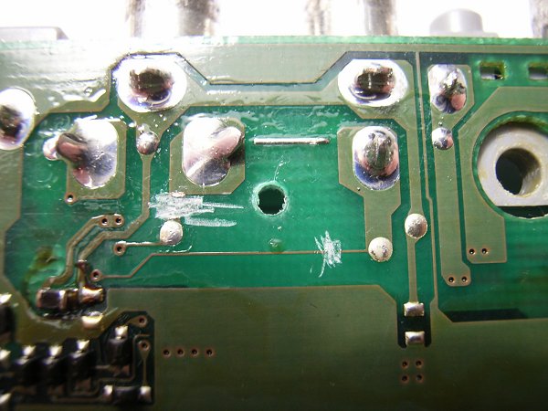
4: Replacing the output stage These are the consequences I have personally drawn from all the results developed in the forum: I believe it is better to fully replace the output stage by a simple highpass filter instead of removing single components. In the procedure shown in the following, the new output stage is connected to the RCA jacks of the PS1. Of course, you can use external jacks. Omit steps 1 and 2 if you do so. Drill a hole into the board between the RCAs and disconnect the RCAs from the internal circuit (by cutting the traces with a small screwdriver). Three cuts are necessary, two on the bottom..... Edit: Depending on the thickness of the wire used (see below), you may have to drill two holes (see lowermost image). |
....and an SMD capacitor on top of the board next to the RCA jack has to be removed. The removal of all connections of the RCA jacks to the internal circuit is necessary to avoid any influence of the latter on the newly added output stage. |
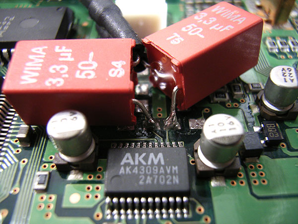
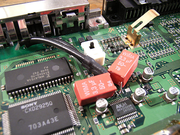
Then I solder two capacitors to the input pads of the first set of caps, i.e. directly to pins 15 and 16 of the DAC. These capacitors act as DC blockers. I used two Wima 3.3uF polyester caps. |
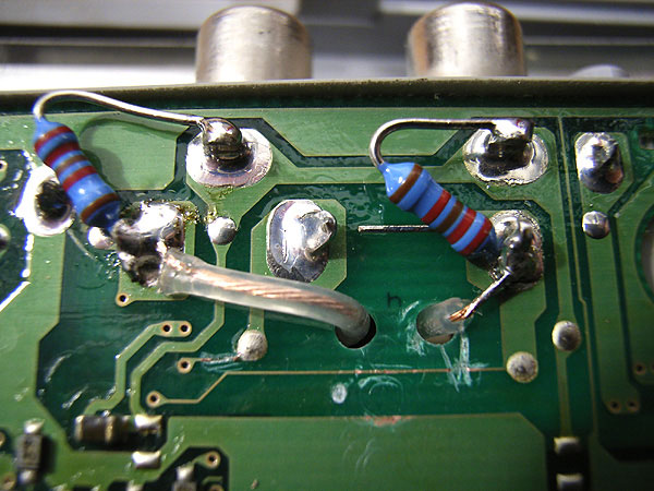
Two wires go from the caps through the hole to the bottom of the board, where they are connected to the + poles of the RCAs. Note that the right-channel RCA has two solder tags for the + pole. Use the leftmost one (as shown in the image) since the other one will be disconnected from the RCA jack when the connector is inserted. (Thanks to Dave Wright aka mrskinny for this information). Finally I soldered a 22k ground resistor directly from the + to the grounds of the RCAs. Edit: While I used laquer wire in a first version of this modification, I here used shielded wires. |
Of course you can use other values for the DC blockers and the ground resistors. Just make sure that the corner frequency of this high-pass filter is well below the audio band, in order to avoid cutoffs in the bass. The corner frequency (-3 dB point) is calculated according to f = 1/(2 x Pi x R x C), where R and C are the values of the ground resistor and DC blocker cap, respectively. The values used here yield a f=2.2 Hz. Note that you have to take the input impedance of the following stage, i.e. your preamp, into account. The corresponding resistors are in parallel, i.e. their values add as R = R1*R2/(R1+R2), where R is the total resistance, and R1 and R2 are the ground resistor of the output stage (22k in this example) and the input resistor of the following stage, respectively. In my setup, for example, I connect the PS1 to a 22 k input impedance of the following stage, which then leads to a total impedance of 11k and a cutoff frequency of 4.4 Hz. |