Stabilized power supply for Chipamps

by Mick Feuerbacher, October 2006.


An alternative discrete approach to the LM338 regulator shown on this site. It is fed by an unregulated power supply unit. I use it with the design shown here.
I acknowledge the work of Pedja Rogic. The stabilizer shown here is based on his excellent design. The differences are the symmetrical use of npn transistors in both rails, different transistors for the Darlingtons, and an additional snubber. On his site, Pedja shows some simulations revealing the very good "PSRR" of the circuit.


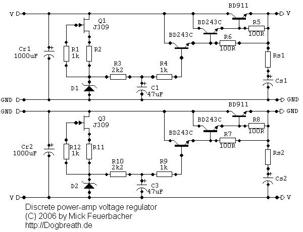
The stabilizer essentially consists of a current source (J309), a Zener diode as voltage reference, and a pass transistor fed by a Darlington.

The source resistors of the JFets (R2 and R11) should be chosen such that the source current amounts to 7 to 9 mA. Which resistance is to be used depends on the Idss of the Zener but should in the range of 100 to 200 R. In my case, 120 R turned out to be appropriate.

The output voltage is Uzener - Ube of the transistors used. Choose the Zener diode accordingly (between 24 and 33 V). The input voltage, i.e. the output of the unregulated feeder supply, should be accordingly higher. I use a supply with 30 V secondaries, i.e. 42 V DC. The Zener diode is a 1N5363 (30 V) type. Under load, the output voltage is 27.8 V.

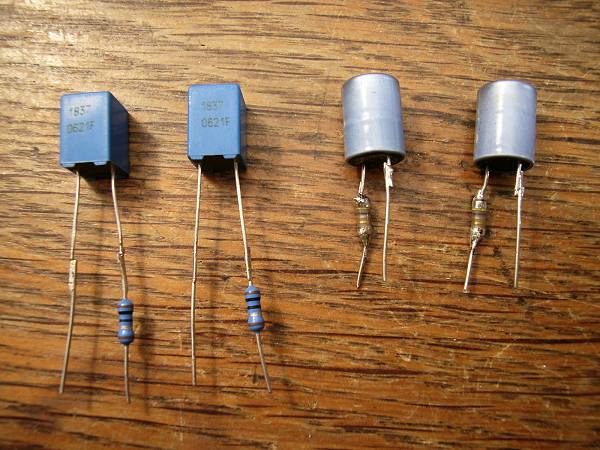
I am still experimenting with the snubber values.

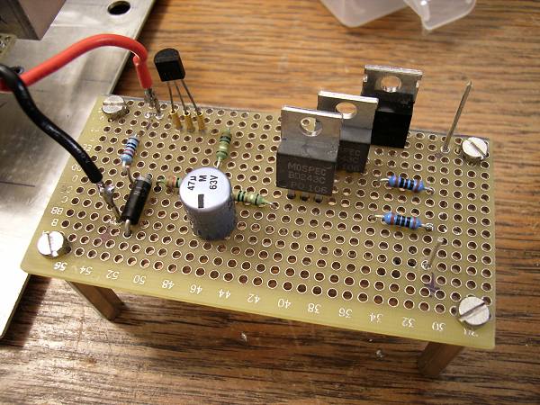
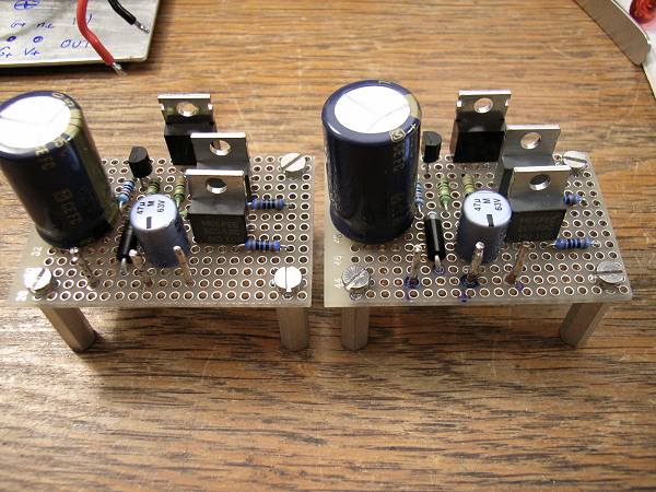
It is understood that you use this stabilizer with additional bypass caps on the supply pins of the chip. Pedja recommends 100 uF for his design, I am currently using it with 2200 uF and 1000 uF. Without the use of additional output caps and/or bypass caps, the regulator may become unstable, particularly when used with slightly inductive loads!

Using a 22 uF output cap I measured an absolutely flat output on my scope (amplitude of residual ripple and noise well below 1 mV). Under varying load, the voltage breaks down only by about 0.2 V (i.e. less than 1 %) between currents of 50 mA and 1.5 A.


It is a good idea to build a test circuit first, in which you can easily swap parts. This is recommended as it is necessary to choose the appropriate source resistor for the JFet, and it may be required to match Zeners (or other parts).


My finished units. They are built much more compact than the test circuit. As can be seen in the schematic, the regulators for the positive and negative rail are identical.


Top view.


Bottom view.


The units in my test jig, which is plugged between the unregulated supply and the amp. The BD911 transistors need a cooler. Whith a cooler as shown, they run at about 35 to 40 °C for normal listening levels.


In the pictures the units are shown without the snubber. For testing I use smal snubber units which I can quickly plug in an out the circuit. After testing the final snubber configuration will be fixed on the board.

The image shows 100 nF/1R (left) and 47uF/0R47 (right) snubbbers.