A minimalistic chip amplifier

by Mick Feuerbacher, July 2006. Updated August 2006, August 2006.


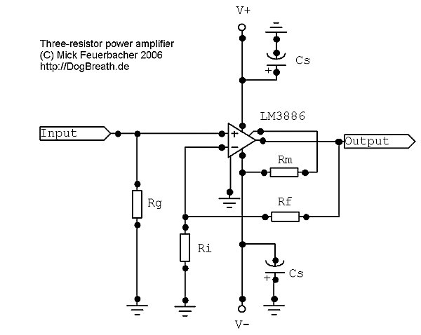
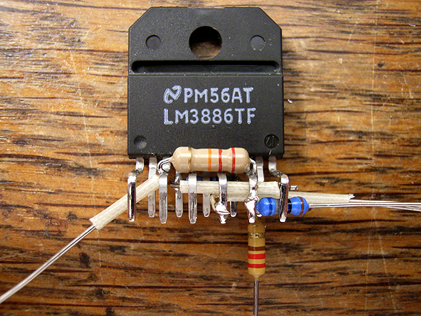
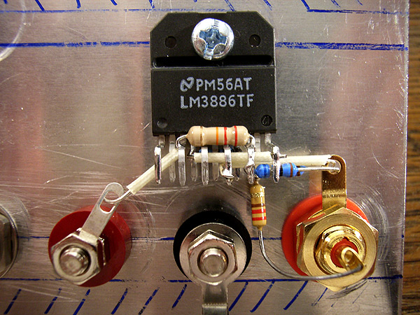
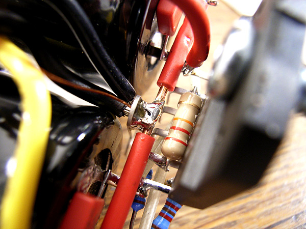
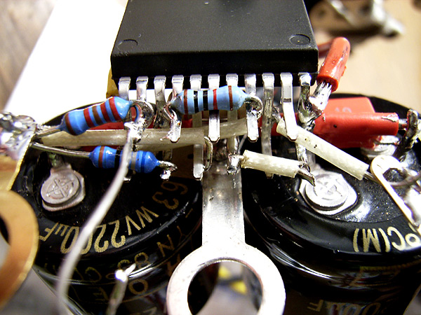
This project is a minimalistic LM3886 based power amplifier. It has only the minimum number of parts in the signal path: Three resistors - nothing else. These three resistors are required for the functionality of the amp so further simplification in this sense is impossible. Referring to the schematic below, the three resistors are Rg, which sets the input impedance of the amp, and Rf and Ri, which set the gain. In particular in this design the use of an input coupling cap is avoided. This greatly improves clarity and transparency, in particular if the preceding stage has output coupling capacitors. These would otherwise be unnecessarily cascaded with the input capacitors, which is not good for the sound. If you want to build this amp, be however careful if you are not sure if the preceding stage in your system has output coupling caps. If it has not, DC may enter the amp, which will be amplified and sent to your speakers! Also, be careful if you have difficult to drive speakers. The amp has no Zobel network or any other stabilizing components.

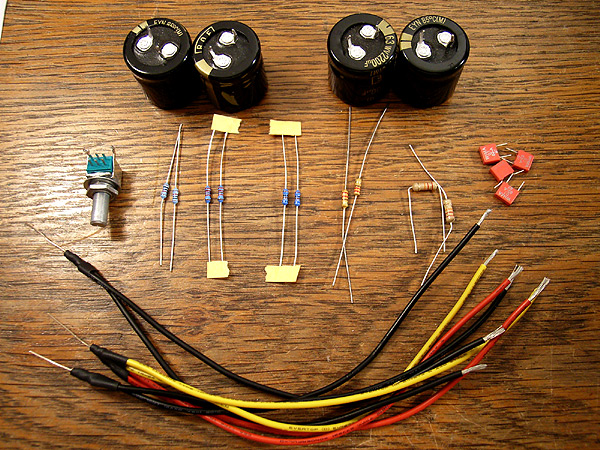
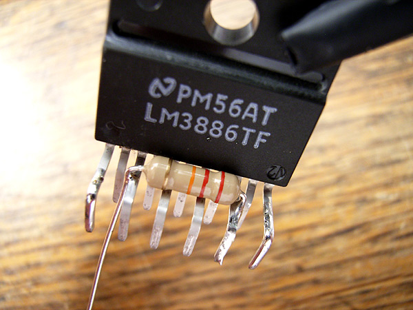
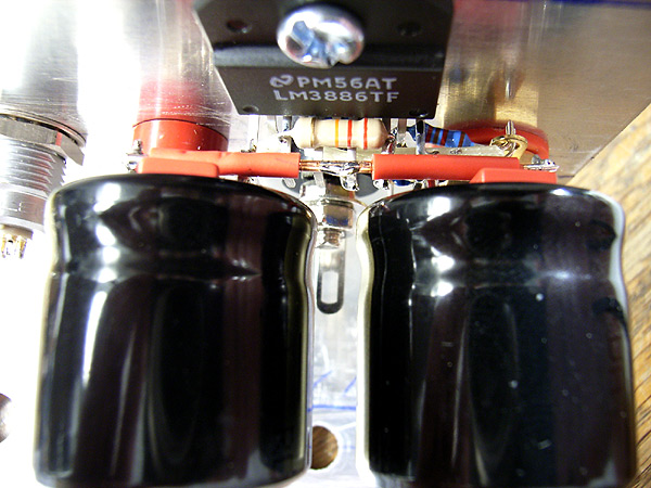
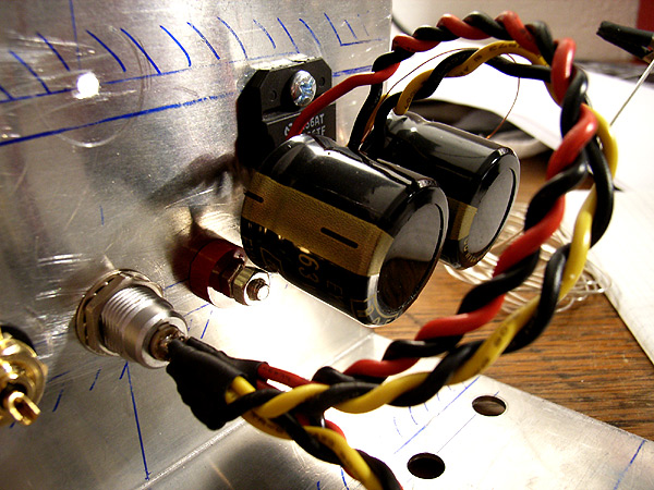
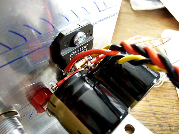
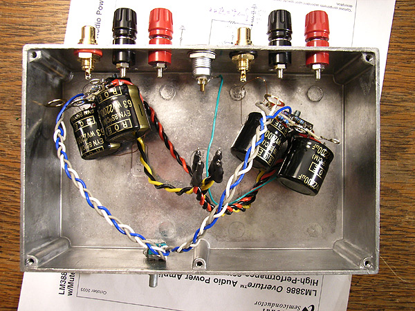
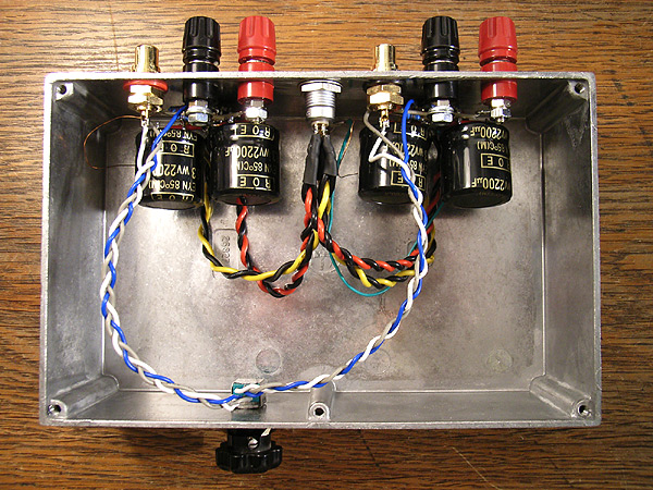
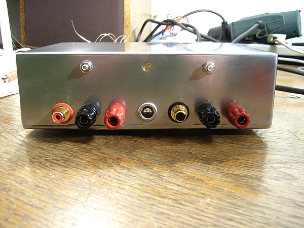
Of course finishing the amp requires additional parts, but these are not in the signal path. The LM3886 has a muting function which requires 
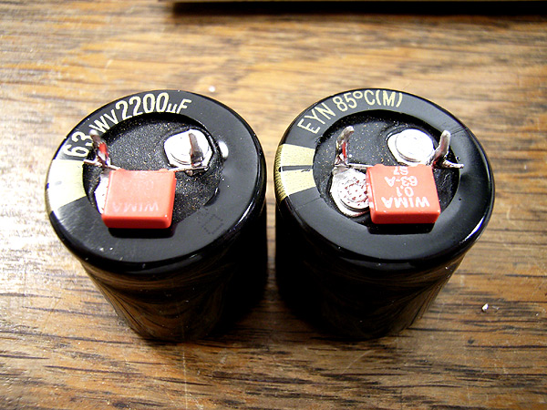
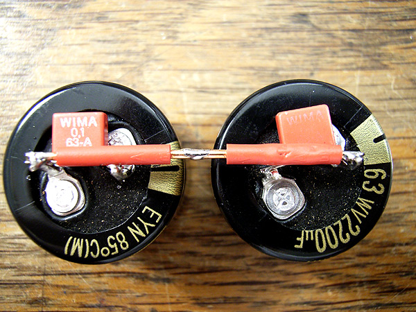
the addition of a resistor Rm to V-. Also power supply bypassing is required, which here was done with a 2200 uF electrolytic parallelled with a 100 nF film capacitor.

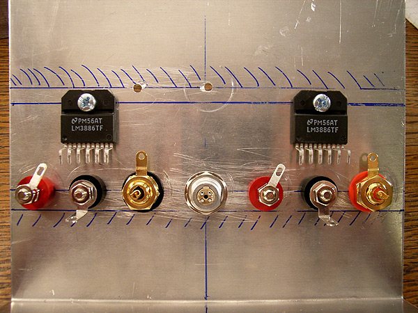
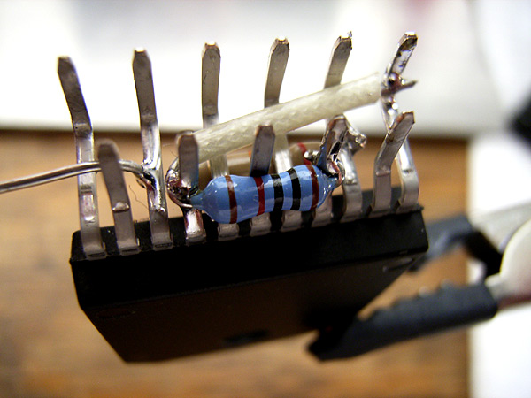
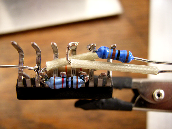
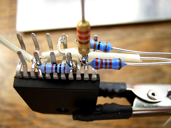
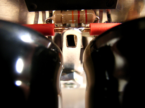
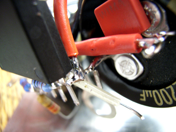
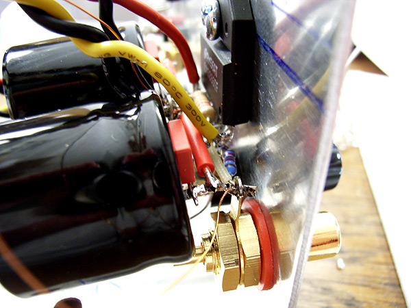
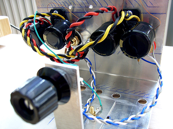
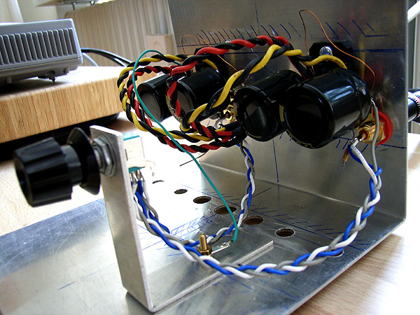
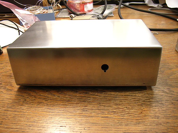
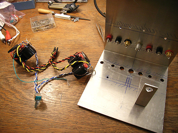
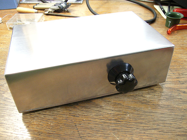
The amp is built point-to-point, i.e. no PCB or matrix board was used. The geometry was chosen according to the following criteria. i) I wanted to have it extremely compact and ii) I minimized the area of any current loops, which lead to unwanted incuded voltages in the circuit.

In the following you find an illustrated description of the build process of my amp. It is rather detailed and step-by-step, which may be helpful for beginners. You are invited to use it as a guide for building your own amp - if you do so, I would be grateful for your feedback..


Fig. 1: This is the schematic of the amp. The chip is a National Semiconductors LM3886.The following additional parts are used:

Part Value Rating, type
Rg 22k 0.35 W metalfilm
Rf 22k 1 W carbon
Ri 680R 0.35W metalfilm
Rm 10k 0.35 W metalfilm
Cs

2200 uF
|| 100 nF

63 V electrolytic;
100 V MKS

Please note that Rf is overrated. This is just my personal choice. The minimum power rating for all resistors is 1/4 W.

The gain is chosen fairly high, it amounts to about 33, which makes it possible to use this amp without a pre. For use with a pre, lower the gain to about 20 by changing Rf or Ri.

Optionally, you can add a resistor in series to the input. This resistor should have something like 220R.


Fig. 2: Before you start building, select the parts you will use. Use a multimeter to match the parts to be used in the left and right channel.

In the back you see the Cs electrolytics, in the middle (from left) the pot (I use an Alps RK09 for testing), the resistors and the bypass caps. On the picture the optional input resistors are also shown. In the front are the wires I use for connection of the amp to the supply terminal.


Fig. 3: Make a careful layout of the position of the parts and the connectors. I always build the amp on a test jig first (I use an aluminum book end), which makes soldering and modifying, if necessary, much easier and the finished amp will be moved to the final case as a whole. On the test jig, the positions of all connectors should be exactly as they later will be in the final case.

As you see, I build my amp identically for both channels, i.e. it is not mirror-symmetric as in most other designs. This way, wiring can be optimized and be done equally efficient for both channels. Note that channel matching is not only important for the parts used, but also involves wire lengths, surroundings for the parts and leads, etc.


Fig. 4: Rf is soldered between pin 3 (out) and 9 (in-). The left connector is not cut as it wil be used to connect the pin to the positive output jack.


Fig. 5: Rm is also soldered directly on the pins (8 to 4). I added a connection from pin 4 (V-) to pin 11 (nc), so that I could make the V- connection there and get a more symmetric layout.


Fig. 6: The signal ground star will be placed on the RCA connector. Therefore Ri and the ground connection are directly soldered on pins 9 and 7, respectively, and the leads on the right are left uncut.


Fig. 7: Here Rg and the optional input resistor is soldered on pin 10.


Fig. 8: The chip with all connections from the front...


Fig. 9: ... and attached to the jig. You can see that I have attached the parts such that they nicely connect to the corresponding connectors.

Note added: Add a jumper connecting pins 1 and 5. See update.


Fig. 10: Now solder the bypass caps directly on the pins of the Cs electrolytics.


Fig. 11: The outer contacts of the Cs caps are connected to a thick copper wire. The copper wire is isolated where it passes the other connectors of the caps, and skinned in the middle, where the power ground will be placed.


Fig. 12: Now connect the caps assembly to pins 1 and 11 of the chip. Make sure that the polarity is correct: The positive connector of the left cap and the negative connector of the right cap are soldered to pin 1 and 11 respectively.

Between the caps you can see the solder tag of the speaker return, which has to be connected to the power ground star.


Fig. 13: At this point I decided to use a straigth solder tag oriented upwards instead of the 90° bent one shown in the previous figure and in figure 3. This allows me do connect it directly to the power ground and to save another piece of cable length.


Fig. 14: V+ is connected to pin 1.


Fig. 15: The power ground star.


Fig. 16: V- is connected to pin 11. Amp completed.


Fig. 17: As you see, the complete amp is very compact. It takes only a few cubic centimeters space. On the lower left you see the supply terminal.


Fig. 18: I use a snubberized supply to power this amp. See a description here.


Fig. 19: The grounding scheme. The mains earth is connected to the PSU case directly. The two ground connections (+ and - grounds) are lead to the amp separately. The cable used for the PSU-amp connection is a shielded four-wire cable. The shield is connected to both the amp and the PSU cases.

The ground connections coming from the PSU are split (left and right channel) in the amp and both are connected to the power star ground of the respective channel. The power stars, as shown below, are connected to the signal stars by a thin wire. One power star is connected to the case.

At each power star the PSU grounds, the speaker return and the connection to the signal star are connected. All other grounds are connected to the signal star.

Note that the separation of signal and power star ground is another deviation from the original Gaincard layout.


Fig. 20: The signal ground is on the minus pole of the RCA connector. The power ground star is seen in Fig. 15. The two star grounds are connected by a thin and relatively long copper wire in order to lift the signal ground by a small amount.
This grounding scheme is done independently for both channels.


Fig. 21: The second channel is now also finished. The green wire you see on the right is the connection of the power ground star to the chassis.


Fig. 22: On the left you see the small pot for testing. Note that I have changed the connection of the optional input caps with respect to Figs. 7 and 8: a longer connector end is attached to the pin, such that I can solder the input wire before or after the resistor itself in order to try the configurations with and without this resistor.

Also note that it is easy to change the amp from integrated to power amp (i.e. with and without a pot). Connect the pot (I to the RCA connector, O to the input resistor lead (see above) and G to the signal star ground for an integrated amp. Or connect the input resistor lead directly to the RCA connector for a power amp.

Before you connect the amp to your system check the DC offset: Connect the speaker outputs to a load (I use a 4R7 10 resistor, power up the amp, and measure the DC voltage across the resistor. In my amp I found about 30 mV for both channels, which is fine. Then connect it to some crap speakers and run it for a while. Only if no problems occur, connect it to your precious speakers.

I should mention that for the first channel I built I used a chip which was damaged. The DC offset was very high (0.3 V) and the sound was distorted in the bass. So I built the amp again using a new chip and it worked fine.


Update August 2006: Pin 1- pin 5


A user at diyforum.com (SpittinLLama) convinced me, with some well founded arguments, that a jumper should be soldered between pins 1 and pin 5 (both +V), as otherwise the full current in the chip is lead over a narrow internal structure.

As I was about to recase my amp anyway, I followed his advice and made a jumper. There was no change in the sonics, but maybe I am more on the safe side concerning the operation of the amp.

The jumper is seen on the lower right side of the amp. I isolated the jumper in order to avoid unwanted contact with pin 2 or 4.


Update August 2006: Recasing


I chose a very simple industrial case as a new home for my amp. It is an Aluminum diecast case (afaik Deltron builds these) of about 18 x 8 x 5 cm.

This is the raw case...


... and here it is after drilling the holes and polishing.


The amp can be removed as a whole from the test jig.


Here it is shown just lying in the new case...


... and after making all connections.


This is the finished amp. The knob was taken from an old piece of electronic equipment.


And from the back. Note the non-mirror symmetric arrangement of the connectors.