A linear regulated power supply unit for the Sony Playstation SCPH100x to SCPH550x: Version 2.

by Mick Feuerbacher, January 2007


The stock Playstation is equipped with a relatively simple switch mode power supply (SMPS). Good modern switch mode supplies can outperform simple linear supplies, but then they have to built with much care. I have noticed some problems with the SMPS in the PS1, however, in particular concerning noise and stability.
In this article I present a linear regulated power supply unit to replace the SMPS. Please note that I previously published another, simpler design, which is easier to build but outperformed by this design.

The power supply of the stock PS1 delivers two voltages: 7.6 V and 3.6 V. It is connected to the main board by a seven-pole connector (see also this article). The pinout is as follows (pin 1 is always the one closest to the front of the PS1):

1: 7.6 V
2: 0 V
3: 3.6 V
4: 0 V
5: 3.6 V
6: 0 V
7: reset

For the design of a new PSU it is also necessary to know how large the currents drawn are. I measured the following values:

1: Startup/Stop 0.8 to 1A; idle 250 mA; play 450 mA
3: always 500 mA
5: no current

The conclusion of this is that the 7.6 supply (pin 1 and its return, pin 2) and the first 3.6 V supply (pin 3 and its return, pin 4) have to be designed for relatively high currents. Pin 5 supplies no current, so it can be omitted as well as its return on pin 6 (yes, you can remove these connections and nothing will happen). The connection on pin 7 can also be omitted - it is not needed for audio, and should your PS1 hang up during operation, you can easily reset it by switching it off and on.
The conclusion is that the new PSU only needs to provide two lines - one for 7.6 V and one for 3.6 V, which are on pins 1 and 2, and on pins 3 and 4, respectively. Btw, the 7.6 V supply is for the motor, the other one feeds the chips. The latter is on the board further regulated for 3.0, 3.5 and 5.0 V supply.

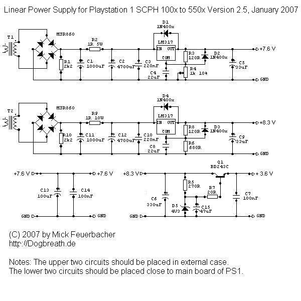
The schematic of the new PSU. I decided to build a single regulation for the 7.6 V line and double regulation for the 3.6 V line. The first regulation steps are done via LM317 regulators. In order to keep the 7.6 V line adjustable, a 1k trimmer is used. It has to be set to about 610R for an output voltage of 7.6 V.
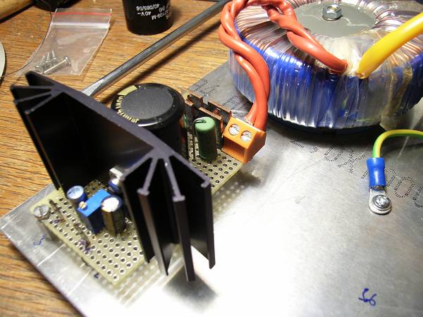
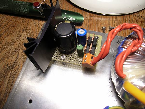
The 8.3 V line does not have a trimmer because it is further regulated anyway. Make sure that the serial regulators R2 and R9, forming low-pass filters with C2 and C12, respectively, are rated high enough. 5 or 10 W types should be used, wirewounds are ok here.

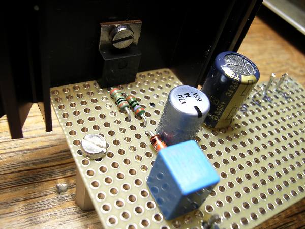
The second regulation step is done via a discrete Zener regulator. A regular 4.3 V Zener diode will, with the Ube voltage drop at Q1, lead to the correct output voltage (the voltage drop over the base-stoper R7 is negligible), You may be forced to try several Zener diodes before you find one which gives the correct voltage drop - they are usually not very precise.

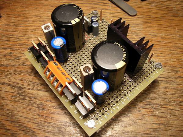
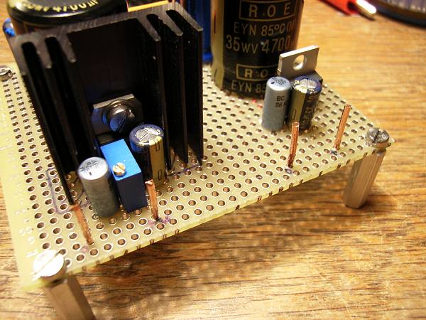
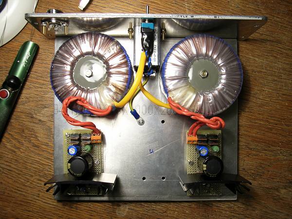
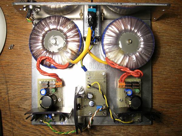
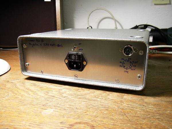
The two lines providing the first regulation step (upper two circuits) should be placed in a separate case (because of the heat created in the LMs and the serial resistors, and because the space in the PS1 is too 
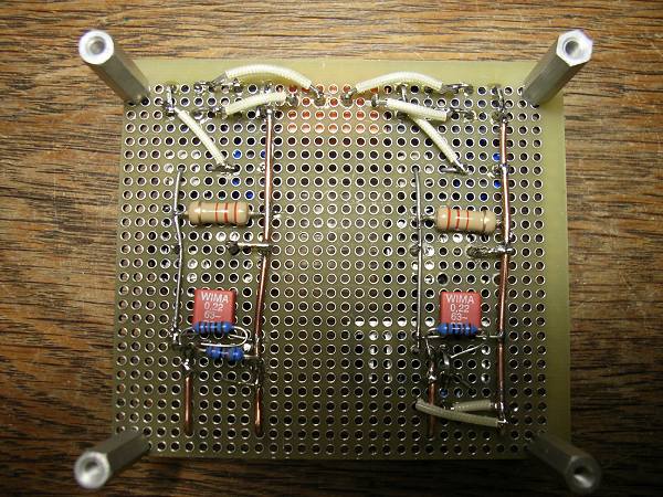
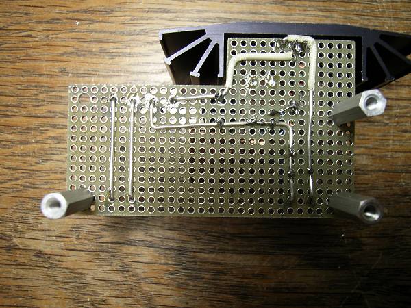
much limited anyway. The second regulation step, however, should take place as close as possible to the main board of the PS1. Build the lower to circuits on a separate board and put them in the free space in the PS1 case, where the stock SMPS was placed. This ensures that the supply is as clean as possible, and noise caught by the umbilical is filtered out at the board.
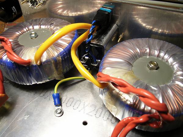
Accordingly, the lower left supply is sort of a "reservoir stage" for the 7.6 V supply line. C12 and C6 at the inputs of these two circuits form another low-pass filter with the resistance of the umbilical ;-)

An early version of the first regulator stages (7.6 and 8.3V). I installed them on one board.

The LM317 regulators. The heatsinks I intended to use were far too small.

The bottom side. All connections are ready but the protection diodes are not yet installed.

The first regulator stages in their case. The picture shows a later version of the unit, where I separated the 7.6V and 8.3V lines because I had to use bigger heatsinks.

As transformers I used 10V/75VA types with a single secondary winding per trafo. They are certainly oversized, but I had them from a succesful dumpster dive. The minium VA rating required is about 8V x 1A for one and 4V x 1A for the other rail, i.e. 12 VA for both rails. Double this for some headroom, i.e. an ordinary 2 x 12 V, 25 to 30 VA trafo may be used.

The 7.6 V line with the larger heat sink.


Between the trafos the (optional) netfilter can be seen.

The second regulator stage for 3.6V

Bottom of the second regulator board.

For testing, I have put the second regulator stage into the same case as the first stage. This way I can do AB testing with the stock SMPS. In a later stage, the second stage (the board in the middle) will be placed in the case of the PS1.


Front side of the external PSU case.

Back side.